
🎓 Request a Quote To Get An EDU Discount
Couldn't load pickup availability
The Agilent ParBERT 81250 is a modular parallel bit error ratio test platform designed for physical layer test and characterization of high-speed multi-port devices. Built on a VXI-based architecture, the system pairs clock modules with interchangeable data, generator, and analyzer modules to deliver a configurable test instrument that addresses everything from synchronous mux/demux devices to clock-synchronous multi-port and multiple serial applications across the computer, communications, and semiconductor industries.
ParBERT 81250 was originally designed to test and characterize synchronous devices such as Mux/Demux components typical of the communications industry, and the platform is equally suited for clock-synchronous multi-port and multiple-serial applications common in the computer industry. The datasheet documents application examples including OC-192 SONET mux/demux test, 10GbE-XAUI characterization, passive optical network (PON) OLT receiver testing, HDMI sink testing, MIPI D-PHY signaling, PCI Express receiver jitter tolerance, and A/D converter characterization using the analyzer's CDR-per-channel feature.
Hewlett-Packard's test and measurement business was spun out as Agilent Technologies in 1999, and the electronic measurement portion of Agilent was subsequently transferred to Keysight Technologies in 2014. ParBERT 81250 instruments shipped under the Agilent brand are part of that lineage, and calibration and service support for many Agilent-era T&M products continues through Keysight's support infrastructure.
The ParBERT 81250 family is organized around a modular architecture in which a VXI mainframe houses one or more clock groups, each consisting of a central clock module and one or more data modules. Within this architecture the datasheet defines three primary speed classes — a 675 Mb/s class, a 3.35 Gb/s class, and a high-speed class covering 7 Gb/s and 13.5 Gb/s — together with three compatible central clock modules (E4805B, E4808A, and E4809A) whose compatibility with the data modules is defined by the supported data rate range.
Module selection is driven by the data rate of the application and the desired channel count. The 675 Mb/s class uses back-end data modules that hold up to four front-ends per slot; the 3.35 Gb/s class uses modules that hold up to two front-ends per slot; the 7 Gb/s and 13.5 Gb/s class uses dedicated single-channel generator or analyzer modules. The datasheet documents that channels within one module can operate at different data rates of binary ratio, and that multiple clock groups can run independently or be locked in an m/n frequency ratio.
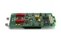
Each pre-owned module and system below is its own dedicated product page with condition-matched pricing. Because ParBERT 81250 is a modular platform, the configuration of clock modules, data modules, and front-ends determines both the channel count and the data rate coverage of a given system — review the specific configuration on each product page to confirm it matches your application.
The principal differences across the family are data rate range, channel density per module slot, and front-end architecture. The 675 Mb/s class (E4832A data module with E4835A analyzer and E4838A generator front-ends) operates from 333 kb/s to 675 Mb/s, holds up to four front-ends per back-end, and addresses LVDS, PECL, ECL, TTL, and 3.3V CMOS I/O. The 3.35 Gb/s class (E4861B data module with E4862B generator and E4863B analyzer front-ends) operates from 20.834 Mb/s to 3.35 Gb/s with up to two front-ends per module and supports LVDS, CML, PECL, ECL, and low-voltage CMOS.
The 7 Gb/s (N4874A generator / N4875A analyzer) and 13.5 Gb/s (N4872A generator / N4873A analyzer) classes are dedicated single-channel modules covering 620 Mb/s to 7 Gb/s and 620 Mb/s to 13.5 Gb/s respectively. Both high-speed classes feature voltage-controlled delay inputs on the generators (±100 ps range with DC–1 GHz modulation bandwidth per the datasheet) for jitter injection, integrated CDR on the analyzers with pre-defined common data rates (including OC-192, 10GbE, Fibre Channel, S-ATA, PCI Express, OC-48, and SAN), 64 Mbit memory depth, and 100 fs delay resolution. Compatible clock modules differ by class: the E4805B supports 675 Mb/s; the E4808A supports 675 Mb/s and 3.35 Gb/s; the E4809A is required for the 7 Gb/s and 13.5 Gb/s modules and also supports 3.35 Gb/s and 675 Mb/s. See the comparison table below for module-by-module specifications.
| Model | Type | Max Data Rate | Channels per Module |
|---|---|---|---|
| E4838A | Generator Front-End | 675 Mb/s | 1 |
| N4872A | Generator | 13.5 Gb/s | 1 |
| N4873A | Analyzer | 13.5 Gb/s | 1 |
| N4874A | Generator | 7 Gb/s | 1 |
Additional differences in specifications beyond the few shown above are not listed here — see each model's full specifications below.
| Parameter | Specification |
|---|---|
| Number of channels | 1, differential |
| Impedance | 50 Ω typ. |
| Data formats | RZ, R1, NRZ, DNRZ |
| Output voltage window | –2.2 to +4.4 V (doubles into open up to max. 5 Vpp) |
| Amplitude/resolution | 0.1 V to 3.50 V / 10 mV |
| Level accuracy | ±3% ± 25 mV typ. after 5 ns settling time |
| Level accuracy @ LVDS/(P)ECL | ±1% ±25 mV typ. after 5 ns settling time |
| Variable transition time range (10 - 90%) | 0.5 to 4.5 ns |
| Transition time accuracy | ±5% ±100 ps |
| Transition time @ LVDS/(P)ECL (20 - 80%) | 0.35 ns typ. |
| Overshoot/ringing | < 7% (< 5% typ.) |
| Jitter, Data mode | < 100 ps peak to peak (80 ps typ) |
| Jitter, Clock mode | 8 ps rms typ. |
| Channel addition | XOR and analog |
| Addressable technologies | LVDS, (P)ECL, TTL, 3.3 V CMOS |
| Installs into | E4832A Data Module |
Please review the Manufacturer's Data Sheet to verify published specifications. Feedback on this webpage is always welcome — please reach out to your Test Architect at any time for questions or concerns. Thank you, we truly appreciate you being our customer.
Model No
Agilent
Condition
Used
Manufacturer
Agilent

30+ Years in Business
Secure Payments
Sell Test Equipments
Knowledgeable Staff
On-site Lab
30+ Years in Business
Secure Payments
Sell Test Equipments
Knowledgeable Staff
On-site Lab
Request A Quote
 Chat Live
 Contact Us
 sales@valuetronics.com
