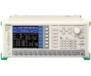
The MG3681A is a Digital Modulation Signal Generator that uses a wideband vector modulator to output the high-accuracy, high-speed vector modulation signals required for R&D and manufacturing of digital mobile communications equipment and related devices. It covers the frequency band of leading mobile communications systems across a range of 250 kHz to 3 GHz, and its vector-modulator architecture delivers excellent frequency response, distortion, and signal-to-noise performance.
Built for digital mobile communications work, the MG3681A performs accurate receiver sensitivity testing and transmitter adjacent channel leakage power testing for high-speed modulation communications systems. It also provides analog modulation functions such as AM and FM for testing analog communications systems, and its signal purity together with functions such as memory and frequency sweep make it useful as a general-purpose signal generator.
ValueTronics stocks and holds its own inventory in a 20,000 sq ft secure warehouse at 1675 Cambridge Drive in Elgin, Illinois. Every used unit we sell is inspected and functionally verified in-house before it ships, while new units ship factory-sealed exactly as received — so buyers get instruments backed by hands-on verification on the pre-owned side and untouched factory condition on the new side.
The MG3681A is a single mainframe built as an expansible platform rather than a fixed-function instrument. Its seven expansion slots, optional reference oscillators, optional AF synthesizer, optional I/Q output function, and optional RF high-level output let a single base unit be configured for a wide span of analog and digital modulation tasks across the 250 kHz to 3 GHz range.
Because the differences between configurations come from installed options, expansion modulation units, and their dedicated software rather than from separate model tiers, the comparison below focuses on how a given MG3681A is equipped — the base mainframe capabilities versus the capabilities added by optional units.
Each pre-owned configuration listed below is its own dedicated product page with condition-matched pricing. Review the specific options and expansion units associated with the unit you are considering, and select the page that matches both the configuration and the pre-owned condition you need.
What distinguishes the MG3681A within its own catalog is the combination of a 30 MHz wideband vector modulator, a 14-bit I/Q waveform data bus across all seven expansion slots, and a synthesizer that reaches a –145 dBc/Hz typical noise floor (above 5 MHz offset) — the basis for its receiver sensitivity and adjacent channel leakage power testing on high-speed modulation systems.
The meaningful differences between MG3681A units are configuration-driven. Internal digital and vector modulation depend on which expansion modulation unit (CDMA, TDMA, Universal, or AWGN) and which software (W-CDMA, IS-95, PDC, GSM, CDMA2000 1xEV-DO, PHS, and related) are installed, and internal analog modulation depends on whether the AF synthesizer option is fitted.
Reference-oscillator options change the aging rate down to 5 x 10⁻¹⁰/day, the I/Q output option adds level, offset, and differential output control, and the RF high-level output option adds 8 dB of gain over 1900 to 2300 MHz. The comparison table that follows reflects these option and expansion-unit configurations rather than separate performance tiers.
| Model | Frequency Range | Output Level | Modulation |
|---|---|---|---|
| MG3681A | 250 kHz to 3 GHz | –143 to +13 dBm | AM, FM, φM, Pulse, Vector |
| MU368010A | — | — | TDMA |
| MU368030A | — | — | Universal |
| MU368040A | — | — | CDMA / W-CDMA |
Additional differences in specifications beyond the few shown above are not listed here — see each model's full specifications below.
| Specification | Value |
|---|---|
| Frequency | |
| Range | 250 kHz to 3000 MHz, Resolution: 0.01 Hz |
| Accuracy | Depends on installed reference oscillator; reference frequency accuracy: ±(5% of FM setting deviation + 5 Hz) for frequency modulation |
| Internal reference oscillator | Aging rate: ±1 x 10⁻⁶/year, Temperature stability: ±1 x 10⁻⁶ (0° to 50°C) |
| External reference input | 10 MHz/13 MHz auto-switching, ±10 ppm, ≥0.7 V(p-p)/50 Ω (AC coupled), BNC connector (rear panel) |
| Buffer output | 10 MHz, TTL level (DC coupled), BNC connector (rear panel) |
| Switching time | ≤20 ms (response time from final command to ±500 Hz of set frequency on GPIB at CW, ALC on, except when setting frequency is crossing over 600 MHz and 1010 MHz) |
| Output Level | |
| Range | –143 to +13 dBm (settable range: –143 to +17 dBm) |
| Unit | dBm, W, dBµV, V (dBµV, V selected terminate/open voltage display) |
| Resolution | 0.01 dB (dBm, dBµV units), 3 digits (W, V units) |
| Frequency response | ±1 dB (CW, ALC on, 0 dBm) |
| Accuracy (CW, ALC on); ≤+13 dBm, ≥–127 dBm | ±1 dB (≤1 GHz), ±2 dB (>1 GHz) |
| Accuracy (CW, ALC on); <–127 dBm | ±2 dB (≤1 GHz), ±3 dB (>1 GHz) |
| Output connector | 50 Ω, N-type connector (front panel) |
| Switching time | ≤50 ms (normal mode), ≤100 ms (safety mode), ≤10 ms (continuous mode); response time from final command to ±0.5 dB of final level on GPIB at CW, ALC on |
| Continuous mode | Level continuously adjustable in set value range of ±10 dB (dBm, dBµV units only); for vector modulation by optional digital modulation unit, continuous mode variance depends on modulation setting |
| Safety mode | Mechanical attenuator decreases level to prevent generation of high-level signal spikes |
| ALC on | Continuous wave or pulse modulation wave (burst wave) with RF On time of 10 µs or more; ALC time constant: Auto, 500 ns, 2.4 µs, 5 µs, 24 µs, 50 µs, 240 µs, 500 µs selectable |
| ALC off | Pulse modulation wave (burst wave) whose RF on time is less than 10 µs; restrict item: without AM; ALC calibration: automatic during ALC Calibration operation and at frequency/level setting change |
| Signal Purity | |
| Harmonics | <–30 dBc |
| Non-harmonic spurious (≤2500 MHz) | <–60 dBc (15 kHz to 300 MHz offset), <–30 dBc (>300 MHz offset); fixed frequency spurious –50 dBc (660, 1320 MHz) |
| Non-harmonic spurious (>2500 MHz) | <–30 dBc (15 kHz to 300 MHz offset) |
| Power line and fan rotation | <–40 dBc (CW, continuous mode: off, ≤0 dBm) |
| SSB phase noise | <–118 dBc/Hz (≥10 MHz, ≤1010 MHz), <–112 dBc/Hz (>1010 MHz) (at CW, 20 kHz offset) |
| AM | |
| Range | 0 to 100% (cannot set internal/external modulation independently), Resolution: 0.1% |
| Modulation frequency response | ≤0 dBm, ALC on, in band of ±1.5 dB based on modulation frequency of 1 kHz |
| Internal modulation | Requires AF synthesizer (Option 21) |
| External modulation | 2 V(p-p) approx., 600 Ω, AC/DC coupled switchable, BNC connector (front panel) |
| Modulation signal polarity | Positive/negative switchable |
| FM | |
| Range | 0 to 1000 kHz (≥10 MHz, ≤1010 MHz), 0 to 2000 kHz (>1010 MHz); cannot set internal/external modulation independently |
| Resolution | 10 Hz (0 to 10 kHz deviation), 100 Hz (10.1 to 100 kHz deviation), 1 kHz (101 to 1000 kHz deviation), 10 kHz (1010 to 2000 kHz deviation) |
| Modulation frequency response | DC to 20 kHz (internal modulation, external modulation DC coupled), 20 Hz to 20 kHz (external modulation AC coupled); in band of ±1 dB based on modulation frequency of 1 kHz |
| Internal modulation | Requires AF synthesizer (Option 21) |
| External modulation | 2 V(p-p) approx., 600 Ω, AC/DC coupled switchable, BNC connector (front panel) |
| Modulation signal polarity | Positive/negative switchable |
| φM | |
| Range | 0 to 6.28 rad (≥10 MHz, ≤1010 MHz), 0 to 12.56 rad (>1010 MHz); cannot set internal/external modulation independently |
| Unit | rad, deg |
| Resolution | rad unit: 0.01 rad, deg unit: 1 deg |
| Modulation frequency response | DC to 20 kHz (internal modulation, external modulation DC coupled), 20 Hz to 20 kHz (external modulation AC coupled); in band of ±1 dB based on modulation frequency of 1 kHz |
| Internal modulation | Requires AF synthesizer (Option 21) |
| External modulation | 2 V(p-p) approx., 600 Ω, AC/DC coupled switchable, BNC connector (front panel) |
| Modulation signal polarity | Positive/negative switchable |
| Wideband AM | |
| Modulation frequency response | DC to 15 MHz (±2 dB bandwidth), DC to 30 MHz (±3 dB bandwidth); external modulation, input level: 0.9 V(p-p), ≥100 MHz, ≤0 dBm, modulation frequency of 1 kHz |
| Internal modulation | Requires digital modulation unit (option) |
| External modulation | ≤1 V(p-p), 50 Ω, BNC connector (front panel), sensitivity: 1 V(p-p) = 100% |
| Pulse Modulation | |
| On/off ratio | >60 dB |
| Rise/fall time | <100 ns (external modulation) |
| Minimum pulse width | <500 ns (external modulation) |
| Pulse repetition frequency | DC to 1 MHz (external modulation, ALC off) |
| Internal modulation | Requires digital modulation unit (option) |
| External modulation | TTL level, positive logic, 50 Ω, BNC connector (front panel) |
| Vector Modulation | |
| Modulation frequency response | DC to 15 MHz (±2 dB bandwidth), DC to 30 MHz (±3 dB bandwidth); external modulation, input level: 0.5 V(rms), ≥100 MHz, ≤0 dBm, modulation frequency of 1 kHz |
| Vector error | ≤2.5%(rms) [external modulation, input level: 0.5 V(rms), ≥100 MHz, ≤0 dBm, 3.84 Msps QPSK modulation] |
| Internal modulation | Requires digital modulation unit (option) |
| External modulation | √(I² + Q²) = 0.5 V(rms), I/Q = ±1.5 V(peak), 50 Ω, BNC connector (front panel) |
| Quadrature degree adjustment function | Adjustment range: ≥±1 deg |
| I/Q change | I, Q signal changeable (RF spectrum invert) |
Important: Reverse power protection: ≤50 W (≤1 GHz), ≤25 W (>1 GHz), ±50 V (DC).
Important: When using the MU368010A, MU368030A and MU368040A expansion units, dedicated software must be installed; some expansion units require installation of dedicated software to enable functionality.
Important: Internal analog modulation (AM, FM, φM) requires the AF synthesizer (Option 21); internal vector, wideband AM and pulse modulation require an optional digital modulation unit (expansion unit). The base mainframe alone supports external modulation only for these functions.
Important: Refer to the separate data sheets for the expansion units, software, and Band Pass Filter.
Recommended pairing: install the MU368040A CDMA Modulation Unit with the MX368041B W-CDMA Software to generate W-CDMA-system modulation signals in the MG3681A.
This pre-owned unit is inspected and functionally verified in-house before it ships and is backed by our pre-owned warranty. To confirm its exact condition, firmware revision, installed options, or included accessories for your application before ordering, contact our Test Architects.
ValueTronics supplies both new and used test and measurement equipment. New units ship factory-sealed, exactly as received from the manufacturer; every used unit is inspected and functionally verified in-house at our 20,000 sq ft secure facility in Elgin, Illinois before it ships. Our Test Architects can help you select the condition, calibration, and configuration that fit your application.
Please review the Manufacturer's Data Sheet to verify published specifications. Feedback on this webpage is always welcome — please reach out to your Test Architect at any time for questions or concerns. Thank you, we truly appreciate you being our customer.
Model No
Anritsu
Condition
Pre-Owned
Manufacturer
Anritsu
Rf_gen_freq
250 kHz to 3 GHz

30+ Years in Business
Secure Payments
Sell Test Equipments
Knowledgeable Staff
On-site Lab
30+ Years in Business
Secure Payments
Sell Test Equipments
Knowledgeable Staff
On-site Lab
Request A Quote
 Chat Live
 Contact Us
 sales@valuetronics.com