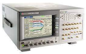
The Keysight J-BERT N4903B is a high-performance serial bit error ratio tester designed for characterizing and stressing chips and transceiver modules that have serial I/O ports operating up to 7 Gb/s, 12.5 Gb/s, or 14.2 Gb/s depending on the configured speed option. As the flagship of the N4900 serial BERT series, the N4903B provides an integrated jitter tolerance test platform that combines a pattern generator with exceptionally low intrinsic jitter, an error detector with built-in clock data recovery, and calibrated jitter sources within a single instrument. The platform can be extended to data rates up to 28.4 Gb/s when paired with a 2:1 multiplexer and demultiplexer with clock data recovery.
The N4903B is positioned for R&D and validation teams characterizing serial I/O ports or ASICs and proving compliance to serial bus standards including PCI Express, SATA, SAS, DisplayPort, USB Super Speed, MIPI M-PHY, SD UHS-II, Thunderbolt, Fibre Channel, QPI, FB-DIMM memory buses, CEI and IEEE backplanes, Infiniband, 10 GbE/XAUI, XFP/XFI, SFP+, and 100 GbE configurations. The integrated jitter sources are specifically designed to address the jitter tolerance compliance requirements of these standards, with an optional library of jitter tolerance curves covering SATA, Fibre Channel, FB-DIMM, 10 GbE/XAUI, CEI 6/11 G, and XFP/XFI.
Keysight Technologies was spun off from Agilent Technologies in 2014, taking with it the electronic measurement business that originated within Hewlett-Packard's test and measurement division before HP separated its T&M operations as Agilent in 1999. The J-BERT N4903B and the broader N4900 serial BERT family carry forward this HP-Agilent-Keysight measurement lineage, and the instrument's remote command set is documented as compatible with the earlier 71612, 81630A Series, and N4900 Series command sets.
| Specification | Value |
|---|---|
| Pattern Generator — Data Output | |
| Range of operation | 150 Mb/s to 14.2 Gb/s (Option D14); 150 Mb/s to 12.5 Gb/s (Option C13/G13, programmable up to 13.5 Gb/s); 150 Mb/s to 7 Gb/s (Option C07/G07) |
| Frequency accuracy | ±15 ppm typical |
| Format | NRZ, normal or inverted |
| Amplitude/resolution | 0.050 V to 1.800 V, 5 mV steps (LVDS, CML, PECL, ECL, low voltage CMOS) |
| Output voltage window | -2.0 V to +3.0 V |
| Predefined levels | ECL (-2V), SCFL (0V), LVPECL (1.3V), LVDS (1.25V), CML (0V) |
| Transition times (20% to 80%) | < 20 ps |
| Transition times (10% to 90%) | < 25 ps |
| Intrinsic jitter | 9 ps pp typical with internal clock (800 fs rms typical) |
| Clock/data delay range | ±0.75 ns in 100 fs steps |
| External termination voltage | -2 V to +3 V |
| Crossing point | Adjustable 20% to 80% typical |
| Skew (data to aux data) | < 15 ps typical |
| Fixed error inject ratios | 1 error in 10^n bits, n = 3, 4, 5, 6, 7, 8, 9 |
| Interface | Differential or single-ended, DC coupled, 50 Ω |
| Connector | 2.4 mm female |
| Clock Output | |
| Frequency range | 150 MHz to 14.2 GHz (Option D14); 150 MHz to 12.5 GHz (Option C13/G13); 150 MHz to 7 GHz (Option C07/G07) |
| Half-rate clocking (Option 003) | Available at bit rates > 2.7 Gb/s; duty cycle adjustable 40% to 60% |
| Amplitude/resolution | 0.050 V pp to 1.800 V pp, 5 mV steps |
| Jitter | 800 fs rms typical with internal clock |
| SSB phase noise | < -75 dBc with internal clock source, 10 GHz at 10 kHz offset, 1 Hz bandwidth |
| Connector | 2.4 mm female |
| Error Detector — Data Inputs | |
| Range of operation | 150 Mb/s to 12.5 Gb/s (Option C13); 150 Mb/s to 7 Gb/s (Option C07) |
| Format | NRZ |
| Max. input amplitude | 2.0 V |
| Termination voltage | -2 V to +3 V or off (true differential mode) |
| Sensitivity | < 50 mV pp (at 10 Gb/s, BER 10^-12, PRBS 2^31-1) |
| Intrinsic transition time | 25 ps typical 20% to 80%, single ended |
| Decision threshold range | -2 V to +3 V in 1 mV steps |
| Phase margin | 1 UI – 12 ps typical |
| Clock-to-data sampling delay | ±0.75 ns in 100 fs steps |
| Interface | Single-ended: 50 Ω nominal; differential: 100 Ω nominal |
| Connector | 2.4 mm female |
| Clock Data Recovery (CDR) | |
| Input data rate | 1 Gb/s to 12.5 Gb/s (Option C13); 1 Gb/s to 7 Gb/s (Option C07) |
| CDR clock output jitter | 0.01 UI rms (RJ) typical with PRBS 2^23-1 |
| Tunable loop bandwidth | 500 kHz to 12 MHz (data rates 1.46 to 12.5 Gb/s); 100 kHz to 4 MHz (data rates 1 to 1.46 Gb/s) |
| Loop bandwidth accuracy | 10% typical (at transition density 50%) |
| Tracking range (SSC) | +0.05% to -0.55% (5500 ppm) deviation of data rate |
| Jitter Sources (with Options) | |
| Periodic Jitter (PJ, Option J10) | 0 to 220 ps pp at all data rates; 0 to 610 ps pp at data rates ≤ 3.375 Gb/s; modulation 1 kHz to 300 MHz |
| Sinusoidal Jitter (SJ, Option J10) | 2 UI at 5 MHz, 1000 UI at 10 kHz; modulation 100 Hz to 5 MHz |
| Random Jitter (RJ, Option J10) | 0 to 15.7 ps rms (0 to 220 ps pp) at data rates < 8.1 Gb/s; bandwidth 50 kHz to 1 GHz; crest factor 14 |
| Bounded Uncorrelated Jitter (BUJ, Option J10) | 0 to 1.1 UI; PRBS 2^n-1, n = 7, 8, 9, 10, 11, 15, 23, 31; PRBS rate 200 Mb/s to 3.2 Gb/s |
| SSC (Option J11) | 0 to -0.5% up/down-spread; 0 to 1.0% pp center-spread; modulation 100 Hz to 100 kHz |
| Sinusoidal Interference (Option J20) | 0 to 400 mV common mode, single ended, differential (0 to 800 mV diff); frequency 10 MHz to 3.2 GHz |
| Pattern Memory | |
| PRBS patterns | 2^n-1 with n = 7, 10, 11, 15, 23, 31; 2^n with n = 7, 10, 13, 15, 23, 31 |
| User definable pattern memory | 32 Mbit, independent for pattern generator and error detector |
| Pattern sequencer | Up to 120 blocks; 1 loop level; loop counter and infinite |
| Mainframe | |
| Display | 8" color LCD touch screen |
| Remote interfaces | GPIB (IEEE 488), LAN, USB 2.0 |
| Other interfaces | Parallel printer port, 2 x LAN, VGA output, 4 x USB 2.0, 1 x USB 1.1 (front) |
| Operating system | Microsoft Windows XP for Embedded Systems (Windows XP Professional for S/N below MY49101000) |
| Operating temperature | 5 to 40 °C (-23 to +104 °F) |
| Storage temperature | -40 to +70 °C (-65 to +158 °F) |
| Operating humidity | 95% relative humidity, non-condensing |
| Power requirements | 100 to 240 V, ±10%, 47 to 63 Hz, 450 VA |
| Dimensions (W x H x D) | 424.5 mm (16.75 in) x 221.5 mm (8.7 in, without feet) x 580.0 mm (22.9 in) |
| Net weight | 26.3 kg (58.0 lb) |
| Shipping weight (max) | 36.3 kg (80.0 lb) |
| Safety | IEC 61010-1:2001; EN 61010-1:2001; CAN/CSA-C22.2 No.61010-1-04; UL 61010-1:2004 |
| EMC | EN 61326:1997 + A1:1998 + A2:2001; IEC 61326:1997 + A1:1998 + A2:2000 |
Please review the Manufacturer's Data Sheet to verify published specifications. Feedback on this webpage is always welcome — please reach out to your Test Architect at any time for questions or concerns. Thank you, we truly appreciate you being our customer.
Model No
Keysight
Condition
Used
Manufacturer
Agilent

30+ Years in Business
Secure Payments
Sell Test Equipments
Knowledgeable Staff
On-site Lab
30+ Years in Business
Secure Payments
Sell Test Equipments
Knowledgeable Staff
On-site Lab
Request A Quote
 Chat Live
 Contact Us
 sales@valuetronics.com